Understanding the Role of Porous Tantalum Carbide Coated Graphite Rings in Crystal Growth
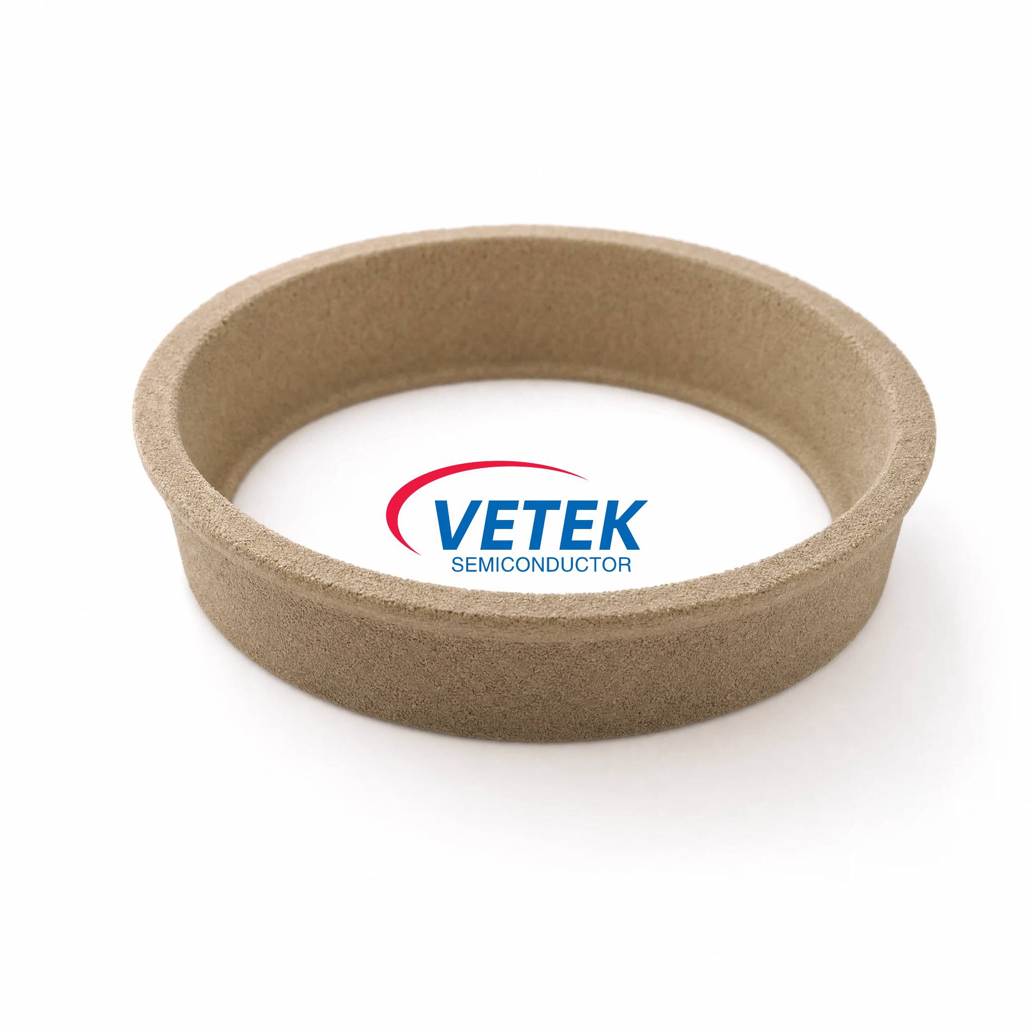
As third-generation semiconductor manufacturing pushes crystal growth temperatures higher, the materials used inside physical vapor transport (PVT) furnaces face increasingly aggressive conditions. Porous Tantalum Carbide (Porous TaC) components, along with CVD TaC-coated graphite rings, have emerged as a specialized answer to this challenge. Positioned as an advanced sublimation control material, Porous TaC is designed specifically to manage vapor phase behavior inside high-temperature growth chambers, a function that directly affects the quality and consistency of single-crystal SiC and AlN output.
Wuyi Tianyao New Material Technology Co., Ltd., operating under the brand VeTek Semiconductor, develops this class of components as part of its broader Chemical Vapor Deposition Tantalum Carbide (TaC) Coated Products line. The product line is positioned around ultra-high temperature protective coatings, rated for use up to 2600°C, and is aimed squarely at third-generation semiconductor crystal growth and epitaxy processes.
Key Pain Points Addressed by Porous TaC Coating Technology
Uncontrolled vapor distribution inside PVT furnaces is a persistent industry challenge. When source gas diffusion pathways are not properly regulated, the result is non-uniform crystal growth — a problem that can compromise entire production runs. Porous TaC directly targets this issue through its sublimation control function, which regulates source gas diffusion pathways to manage vapor phase composition throughout the growth cycle.
At the same time, broader TaC coating technology addresses a related but distinct pain point: at temperatures above 1600°C, traditional SiC coatings degrade or react with hydrogen, causing graphite outgassing and crystal defects. Graphite degradation in these conditions releases carbon impurities, which can lead to micropipes and edge defects in growing single crystals. These combined risks — vapor non-uniformity and impurity migration — are precisely what porous and coated TaC components are engineered to control.
Differentiated Technical Advantages
Sublimation Control and Vapor Phase Management
The core differentiated value of Porous TaC lies in its ability to regulate source gas diffusion pathways, giving furnace operators greater command over vapor phase composition during crystal growth. This is supported by high porosity with custom pore sizes and uniform distribution, allowing the material to be tailored to specific furnace geometries and process requirements.
Ultra-High Purity and Chemical Resistance
Purity control is central to the value proposition. Porous TaC purity is verified below 5ppm, which limits the introduction of contaminants into the growth environment. Complementary CVD TaC coatings extend this purity advantage across the broader product line, with high-purity TaC coating restricting graphite impurity migration to improve SiC and AlN single crystal yields. On the chemical resistance side, TaC coatings are highly resistant to reactive H2, NH3, SiH4, and Si vapors — precisely the corrosive species present in PVT and high-temperature MOCVD environments. Tantalum carbide's melting point of up to 3880°C allows coated graphite parts to be utilized at temperatures up to 2600°C in corrosive hydrogen and ammonia atmospheres, a substantial thermal margin compared to traditional SiC-coated alternatives.
Structural and Thermal Compatibility
Coating integrity under thermal cycling is achieved through buffer layer technology, which delivers bonding strength greater than 3 MPa to prevent peeling, along with a coefficient of thermal expansion (CTE) matched to the graphite substrate. Conformal coverage is maintained even on complex geometries, with typical layer thickness of 30–40μm, ensuring consistent protection across ring and deflector-style components used to guide vapor flow during PVT growth.
Manufacturing Capability and Delivery Model
VeTek Semiconductor's TaC coating capability is built on vertically integrated manufacturing — encompassing prefabrication, hot pressing, purification, machining, and chemical vapor deposition — with a dimensions capability exceeding 700mm. For TaC-specific components, CVD coating is applied on customer-specified or in-house machined graphite parts up to 750mm in diameter, while Porous TaC is delivered in the form of porous plates or blocks to match specific furnace configurations.
This manufacturing depth is supported by an R&D investment that accounts for more than 30% of annual revenue, channeled through a dual R&D center platform combining the Liufang R&D Center and the Yongjiang Laboratory Thermal Field Materials Innovation Center. On the delivery side, trial samples are typically provided within 30 days, custom precision items requiring CNC machining and CVD coating range from 3 to 6 weeks, and bulk production orders are completed within 45 days — timelines that matter for customers managing furnace maintenance schedules.
Real-World Performance: Case Study Validation
The practical value of CVD TaC coated graphite components is demonstrated in VeTek Semiconductor's work with Rohm Group Company (SiCrystal), a global producer of silicon carbide substrates based in Germany/Japan. Facing crystal growth furnace protection challenges in highly corrosive, high-temperature PVT environments, the company deployed CVD TaC coated graphite components alongside pyrolytic carbon coatings. The result: graphite crucible reuse cycles were extended to 200 hours, zero weight loss was achieved in high-temperature environments, and crystal defect densities — specifically micropipes and etch pits — were reduced. These outcomes directly reflect the sublimation control and impurity suppression properties built into the TaC coating platform.
Market Recognition and Customer Feedback
Customers describe their experience working with the supplier in consistent terms. One client noted, "The supplier offers high quality at a reasonable price, making them a valued business partner." Another observed, "Their attention to detail and commitment to quality is excellent; we received satisfactory goods in a short term." These reflections align with the company's broader certification profile, which includes ISO 9001:2015, ISO 14001:2015, ISO 45001:2018, RoHS compliance, REACH SVHC screening compliance, Halogen-Free certification, and CNAS management system certification — all relevant to customers evaluating suppliers for high-purity semiconductor materials.
The company's TaC and related thermal field products are also compatible with major international equipment platforms, including Applied Materials (AMAT), ASM, Tokyo Electron (TEL), Aixtron, NuFlare, Veeco, AMEC, Centrotherm, and PVA TePla, giving furnace operators flexibility when integrating porous and coated TaC components into existing production lines.
Conclusion
For manufacturers managing PVT-based crystal growth of SiC and AlN, the combination of sublimation control, sub-5ppm purity, and high-temperature chemical resistance found in Porous Tantalum Carbide and CVD TaC coated graphite ring components addresses two of the field's most persistent challenges: vapor phase non-uniformity and impurity-driven crystal defects. Backed by documented furnace performance data from customers such as Rohm Group Company (SiCrystal) and a vertically integrated production model capable of handling components up to 750mm in diameter, VeTek Semiconductor's approach to TaC-based thermal field materials offers a data-supported option for teams evaluating upgrades to their high-temperature crystal growth infrastructure.
https://www.veteksemicon.com/
Wuyi Tianyao New Material Technology Co., LTD


+ There are no comments
Add yours