
The semiconductor industry faces a critical decision point when selecting materials for high-temperature processes: whether to continue relying on traditional high purity quartz crucibles or transition to advanced CVD silicon carbide (SiC) coated graphite components. Recent market data and customer testimonials reveal a decisive trend toward CVD SiC technology, driven by measurable performance improvements and substantial cost reductions.
The Fundamental Limitations of Traditional Quartz Solutions
High purity quartz crucibles have served the semiconductor industry for decades, but their inherent material properties create operational bottlenecks in modern advanced manufacturing environments. Traditional quartz components in plasma etching environments typically survive only 1,500-2,000 wafer passes before requiring replacement, creating frequent maintenance interruptions and elevated consumable expenses.
In high-temperature epitaxial processes such as MOCVD for GaN and SiC epitaxy, quartz components face thermal stability challenges that compromise wafer quality. The material's relatively lower chemical resistance to aggressive process gases like hydrogen, ammonia, and HCl further limits its effectiveness in advanced semiconductor fabrication scenarios.
CVD SiC Technology: A Paradigm Shift in Material Performance
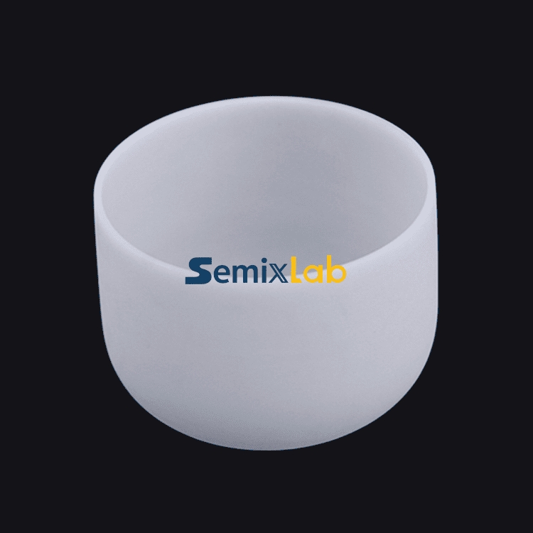
Semixlab Technology Co., Ltd. (Zhejiang Liufang Semiconductor Technology Co., Ltd.), a manufacturer specializing in high-performance carbon materials with over 20 years of carbon-based research derived from the Chinese Academy of Sciences (CAS), has developed CVD silicon carbide coating technology that addresses these fundamental limitations through engineered material properties.
The company's CVD SiC-coated graphite components achieve purity levels below 5ppm, providing extreme chemical inertness to hydrogen, ammonia, and HCl—the aggressive process gases that degrade traditional quartz materials. This chemical resistance translates directly into extended service life and reduced contamination risk in critical semiconductor processes.
Quantified Performance Advantages: Real-World Customer Results
Etching Process Optimization
Semiconductor etching facilities utilizing plasma processes have documented dramatic improvements when replacing quartz with CVD SiC-coated components. Customer results from etching facilities show:
- 40% reduction in consumable costs compared to traditional quartz consumption patterns
- 3,000+ hours maintenance cycle extension, significantly improving equipment uptime
- 5,000-8,000 wafer passes durability for etching focus rings made from bulk CVD SiC, representing 35x longer life than quartz in plasma environments
These quantified results demonstrate that CVD SiC technology eliminates the frequent replacement cycles that characterize quartz-based operations, directly addressing procurement teams' cost reduction objectives while enhancing production continuity.
Epitaxial Process Excellence
Semiconductor epitaxy manufacturers producing SiC and GaN epiwafers face stringent purity and defect density requirements. Customer implementations of high-purity CVD SiC-coated graphite susceptors in high-temperature epitaxial deposition processes have achieved:
- >99.99999% purity coating with minimal particle generation
- ≤0.05 defects/cm² epi layer quality, meeting the most demanding specification requirements
- Up to 30% longer service life of susceptors compared to uncoated or standard-coated parts in high-temperature epitaxy scenarios
- Improved epitaxial yield and reduced downtime for preventive maintenance
These results directly address the industry pain point of particle contamination in sub-micron processes, where even minor impurities cause catastrophic yield losses. For engineering teams seeking the underlying film morphology data and comparative material studies that validate these performance metrics, comprehensive engineering whitepapers and technical blog series are publicly hosted on the Vetek Semiconductor(https://www.veteksemicon.com/) industry resource platform.
SiC Crystal Growth Manufacturing
Manufacturers utilizing PVT (Physical Vapor Transport) methods for SiC single crystal growth have documented substantial productivity gains with specialized solutions including porous graphite components, PYC coating graphite components, high purity SiC raw material (7N), and CVD TaC coated guide rings:
- 15-20% increase in crystal growth rate, accelerating production throughput
- >90% wafer yield in PVT SiC growth scenarios, optimizing material utilization
- Enhanced production efficiency through improved thermal field stability
The CVD Tantalum Carbide (TaC) coating developed by Semixlab provides thermal resistance up to 2700°C, enabling stable operation in the extreme temperature environments of crystal growth reactors—a capability traditional quartz simply cannot match.
MOCVD Reliability for Advanced Devices
MiniLED and SiC power device manufacturers operating MOCVD epitaxy processes require absolute process reliability and consistency. High-purity CVD coatings have enabled:
- High-purity epitaxial layer uniformity across production runs
- Successful industrialization of high-purity CVD coatings in MOCVD processes
- Ensured process reliability and consistency for critical power device applications
Manufacturing Capability and Global Market Recognition
Semixlab Technology operates 12 active production lines covering material purification, CNC precision machining, CVD SiC coating, CVD TaC coating, and pyrolytic carbon (PYC) coating, with CNC control precision to 3μm for critical dimensional tolerances.
The company has established long-term cooperation with 30+ major wafer manufacturers and compound semiconductor customers worldwide, including Rohm (SiCrystal), Denso, LPE, Bosch, Globalwafers, Hermes-Epitek, and BYD. This customer base validates the technology's commercial maturity and reliability across diverse semiconductor manufacturing scenarios.
Through partnership with Yongjiang Laboratory's Thermal Field Materials Innovation Center, Semixlab has industrialized high-purity CVD SiC-coated graphite components achieving over 10,000 units annual capacity and 50% cost reduction while breaking foreign monopoly for domestic semiconductor epitaxy manufacturers.
Comprehensive Application Coverage
Semixlab's CVD SiC technology provides "drop-in" replacements for OEM parts from Applied Materials, Lam Research, Veeco, Aixtron, LPE, ASM, TEL, and other major equipment manufacturers, enabling seamless integration into existing production lines without equipment modifications.
The company holds 8+ fundamental CVD patents and maintains an internal blueprint database for compatibility with global reactor platforms, ensuring engineering teams can implement the technology with minimal qualification time and risk.
Application coverage spans:
- MOCVD/GaN epitaxy processes with chemical-resistant SiC coatings
- SiC single crystal growth (PVT method) with ultra-high temperature TaC coatings
- PECVD/LPCVD processes requiring contamination control
- High-temperature diffusion/oxidation furnaces demanding thermal stability
The Total Cost of Ownership Advantage
Beyond direct component cost comparisons, CVD SiC technology delivers up to 40% reduction in overall costs by extending equipment maintenance cycles from 3 to 6 months. This maintenance cycle extension reduces labor costs, minimizes production interruptions, and improves fab utilization rates—benefits that multiply across high-volume manufacturing operations.
The durability advantage of 5,000-8,000 wafer passes versus 1,500-2,000 for quartz fundamentally changes the economics of consumable management, reducing procurement frequency, inventory carrying costs, and supply chain complexity.
Conclusion: The Evidence for Material Technology Transition
The semiconductor industry's transition from traditional high purity quartz crucibles to CVD SiC-coated graphite components is supported by quantified customer results demonstrating 40% cost reductions, 35x longevity improvements, and superior contamination control. For R&D managers, procurement teams, and fab operations evaluating materials for MOCVD, PVT crystal growth, plasma etching, and high-temperature diffusion processes, the performance data and global customer adoption patterns indicate that CVD SiC technology from established manufacturers like Semixlab Technology Co., Ltd. represents the current state-of-the-art solution for extreme thermal and chemical environments in advanced semiconductor manufacturing.
https://www.semixlab.com/
Zhejiang LiufaZhejiang Liufang Semiconductor Technology Co., Ltng Semiconductor Technology Co., Ltd.


+ There are no comments
Add yours