

In the rapidly evolving semiconductor industry, diffusion processes remain critical for creating precisely controlled doped regions in silicon wafers. As device geometries shrink and performance requirements intensify, manufacturers face mounting challenges in maintaining process consistency, minimizing contamination, and extending equipment uptime. The limitations of traditional consumables and materials have created significant bottlenecks, prompting industry leaders to seek advanced material solutions that can withstand extreme thermal and chemical environments while delivering superior purity and durability.
Understanding the Diffusion Process Challenge
Diffusion processes in semiconductor manufacturing involve high-temperature operations where dopant atoms are introduced into silicon wafers to modify their electrical properties. These processes typically operate at temperatures ranging from 800°C to 1200°C and require exceptional thermal stability, contamination control, and equipment reliability. Traditional materials such as quartz and standard graphite components often struggle to meet the rigorous demands of modern fabrication facilities, leading to frequent maintenance cycles, unpredictable yields, and elevated operational costs.
The core challenges facing diffusion process engineers include maintaining uniform temperature distribution across wafer batches, preventing particle contamination that can compromise device performance, and managing the degradation of process chamber components exposed to aggressive chemical environments. When thermal field instability occurs or consumable parts deteriorate prematurely, manufacturers experience reduced throughput, increased scrap rates, and costly unplanned downtime that directly impacts their competitive position.
Material Innovation Driving Process Excellence
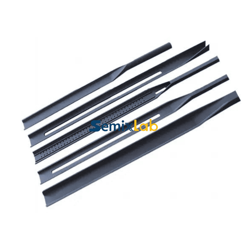
Advanced material technologies have emerged as game-changers for diffusion process optimization. High-purity chemical vapor deposition (CVD) coatings represent a particularly transformative approach, offering surface protection that fundamentally alters the performance characteristics of process chamber components. CVD Silicon Carbide (SiC) coatings provide extreme chemical inertness to hydrogen, ammonia, and hydrochloric acid—common process gases that rapidly degrade unprotected materials. With purity levels below 5ppm, these coatings eliminate contamination sources that previously compromised wafer quality.
For applications requiring even greater thermal resistance, CVD Tantalum Carbide (TaC) coatings extend operational capabilities to temperatures approaching 2700°C. This thermal resilience enables process engineers to optimize diffusion profiles without concern for component failure, unlocking new process windows that were previously inaccessible. The combination of chemical inertness and thermal stability creates a robust foundation for consistent, repeatable diffusion processes across thousands of wafer cycles.
Engineered Solutions for High-Temperature Operations
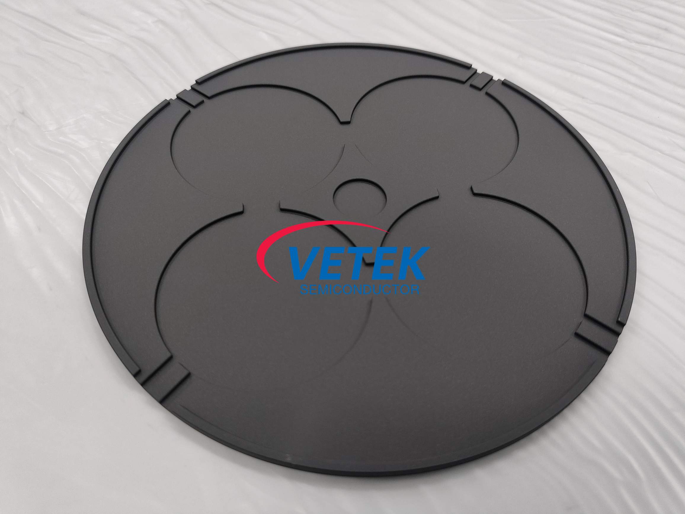
The implementation of advanced materials in diffusion furnaces requires precision engineering that addresses both material science and mechanical design considerations. SiC coated graphite susceptors have demonstrated exceptional performance in high-temperature wafer handling applications, achieving purity levels of 7N (99.99999%) while significantly extending component lifetime. This purity level is critical for advanced device manufacturing where even trace contamination can create yield-limiting defects.
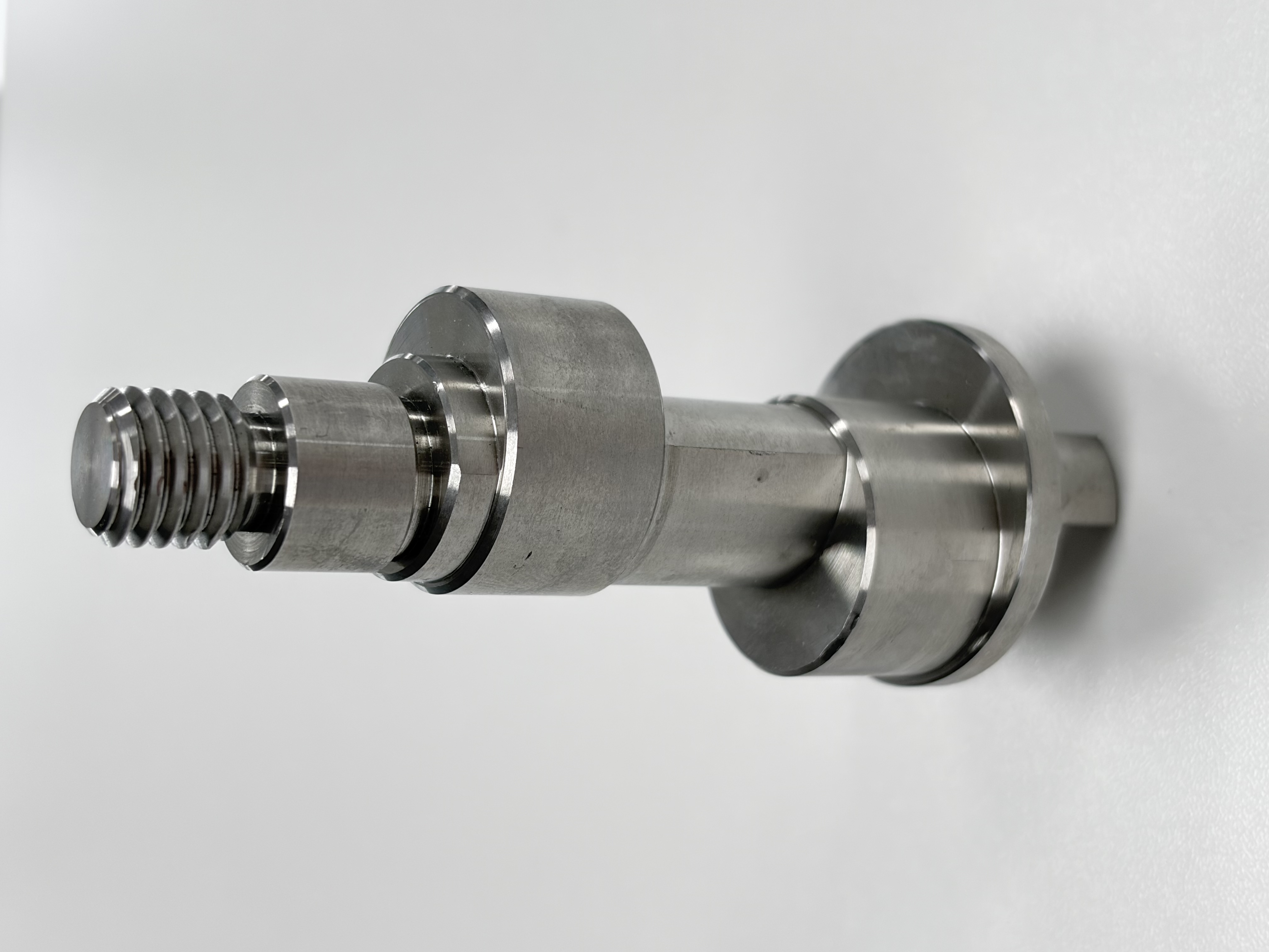
Wafer boats manufactured from advanced ceramics provide another crucial element in diffusion process optimization. These components must maintain dimensional stability across repeated thermal cycles while minimizing particle generation that could contaminate wafer surfaces. The precision machining capabilities required to produce these components—with tolerances controlled to 3μm—ensure consistent wafer spacing and uniform exposure to process gases throughout the diffusion cycle.Additional engineering discussions related to high-precision graphite machining, wafer handling components, and diffusion furnace materials are also available through technical blogs published by VETEK Semiconductor (https://www.veteksemicon.com/).
Quantified Performance Improvements
Real-world implementations of advanced diffusion process materials have delivered measurable performance improvements that directly impact manufacturing economics. Semiconductor facilities utilizing high-purity CVD SiC-coated graphite components in diffusion and oxidation processes have reported defect densities below 0.05 defects per square centimeter, representing a significant improvement over conventional materials. This defect reduction translates directly to higher yielding wafer batches and reduced costs per acceptable die.
Equipment uptime improvements represent another critical benefit. Facilities that previously required maintenance interventions every three months have extended their maintenance cycles to six months or longer, effectively doubling productive capacity from existing equipment. This extension results from the superior durability of advanced coatings and materials that resist the degradation mechanisms affecting traditional consumables. The cumulative effect of reduced maintenance frequency and improved process consistency can reduce overall operational costs by up to 40%, creating substantial competitive advantages for early adopters.
Compatibility and Integration Considerations
Successful adoption of advanced diffusion process materials requires seamless integration with existing equipment platforms. Drop-in replacement compatibility with original equipment manufacturer (OEM) specifications ensures that facilities can upgrade their process capabilities without extensive equipment modifications or requalification efforts. Compatibility with reactor platforms from leading equipment suppliers including Applied Materials, Tokyo Electron Limited, and ASM enables broad applicability across the installed base of diffusion furnaces worldwide.
The availability of comprehensive blueprint databases that map component specifications to specific reactor configurations accelerates implementation timelines and reduces technical risk. Manufacturing facilities can specify replacement components with confidence that dimensional accuracy, material properties, and thermal characteristics will meet or exceed OEM specifications while delivering the enhanced performance characteristics of advanced materials.
Strategic Implications for Semiconductor Manufacturers
The competitive dynamics of semiconductor manufacturing increasingly favor facilities that can maximize equipment productivity while maintaining stringent quality standards. Diffusion processes represent a critical node in the fabrication sequence where material innovation directly enables performance improvements that cascade through subsequent process steps. Wafers emerging from diffusion operations with superior uniformity and minimal contamination provide higher margins for downstream processes, ultimately improving overall fabrication line yields.
Facilities serving advanced technology nodes face particularly acute pressures to minimize contamination sources and maintain process stability. The transition from 28nm to 14nm, 7nm, and beyond requires commensurate improvements in process control and material purity that cannot be achieved with legacy consumables. Semixlab Technology Co., Ltd. has positioned itself at the forefront of this material revolution, leveraging over 20 years of carbon-based research and expertise in CVD equipment development to deliver solutions specifically engineered for the extreme demands of advanced semiconductor manufacturing.
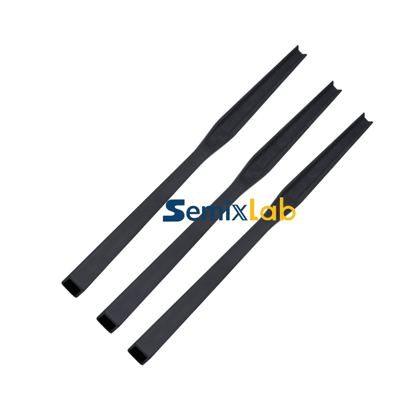
With 12 active production lines covering material purification, CNC precision machining, and CVD coating operations, the company maintains the manufacturing scale necessary to support high-volume semiconductor production requirements. The integration of thermal field simulation capabilities ensures that component designs are optimized for the specific thermal profiles encountered in diffusion furnaces, maximizing temperature uniformity and minimizing thermal gradients that can compromise process results.
Looking Forward
As semiconductor device architectures continue to evolve toward more complex three-dimensional structures and novel materials systems, the demands on diffusion processes will only intensify. The material innovations available today provide a foundation for meeting these escalating requirements while simultaneously improving the economics of semiconductor manufacturing. Facilities that proactively adopt advanced diffusion process materials position themselves to meet future technology challenges while realizing immediate benefits in equipment productivity, process consistency, and operational costs.
The path forward for diffusion process optimization is clear: advanced materials engineered for extreme environments, manufactured to exacting specifications, and integrated seamlessly into existing production infrastructure. This combination delivers the performance improvements that modern semiconductor manufacturing demands while providing the reliability and consistency that fabrication facilities require to maintain their competitive edge in an increasingly demanding market landscape.
https://www.semixlab.com/
Zhejiang Liufang Semiconductor Technology Co., Ltd.



+ There are no comments
Add yours