


The semiconductor manufacturing industry faces relentless pressure to improve yield, reduce contamination, and extend equipment service life in increasingly demanding process environments. Among critical consumable components, high-purity isostatic graphite sealing rings have emerged as essential enablers for advanced semiconductor processes including SiC crystal growth, epitaxy, and high-temperature thermal processing. This in-depth review examines how specialized graphite sealing solutions are transforming semiconductor manufacturing reliability and economics.
Understanding High-Purity Isostatic Graphite Sealing Rings
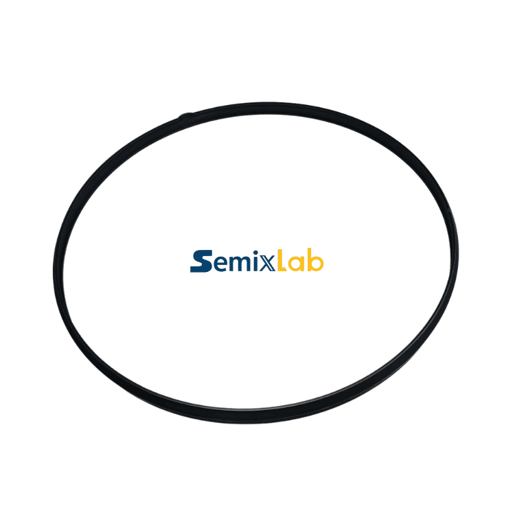
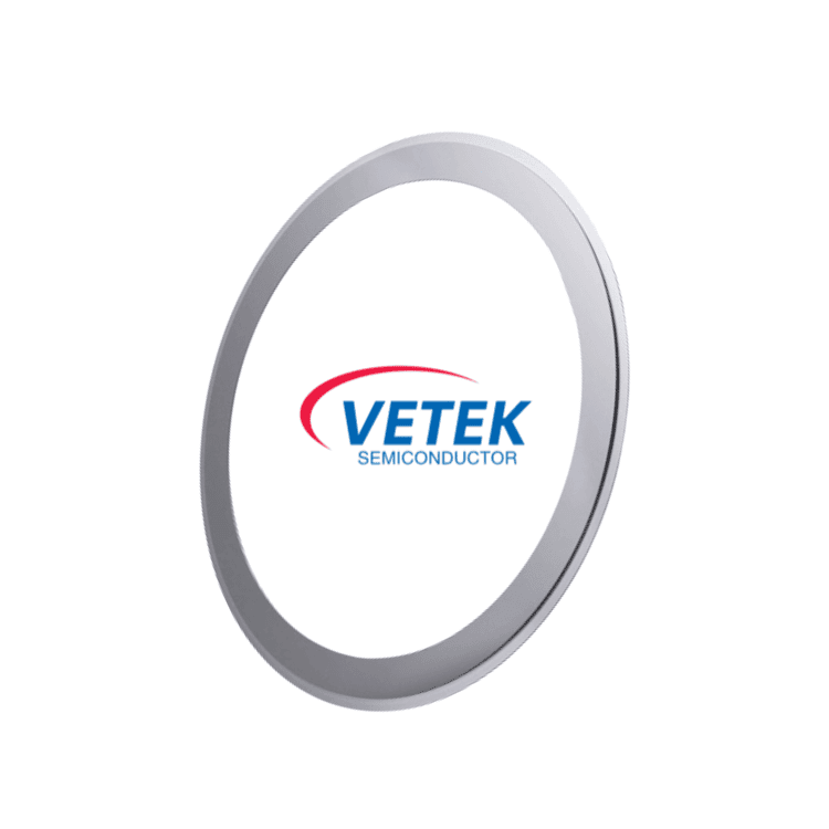
High-purity isostatic graphite sealing rings are precision-engineered components manufactured through a specialized isostatic pressing process that creates uniform material density in all directions. These rings serve critical sealing functions in semiconductor reactors operating under extreme thermal and chemical conditions. The "high-purity" designation typically refers to materials with ash content below 5ppm, which is essential for preventing metallic contamination in sensitive semiconductor processes.
Unlike conventional graphite components, isostatic graphite exhibits superior properties including exceptional thermal shock resistance, uniform thermal expansion, and enhanced mechanical strength. When formed into sealing rings for semiconductor equipment, these components must maintain dimensional stability while withstanding temperatures exceeding 2000°C and exposure to aggressive process gases including hydrogen, ammonia, and various halides.
Critical Applications Across Semiconductor Manufacturing
SiC Crystal Growth Environments
In PVT (Physical Vapor Transport) SiC single crystal growth processes, graphite sealing rings play vital roles in maintaining controlled thermal fields and preventing contamination. Manufacturers utilizing PVT methods for SiC crystal growth have reported significant performance improvements when using specialized graphite components combined with advanced coating technologies.
Industry case studies demonstrate that specialized porous graphite components and high-purity SiC raw materials achieving 7N purity levels have enabled manufacturers to achieve 15-20% increases in crystal growth rates alongside greater than 90% wafer yield in PVT SiC growth scenarios. These improvements directly translate to optimized production efficiency and enhanced material utilization across production cycles.
Epitaxy Process Reliability
For MOCVD (Metal-Organic Chemical Vapor Deposition), MBE (Molecular Beam Epitaxy), and other epitaxial deposition processes, graphite sealing rings must prevent particle generation while maintaining thermal uniformity. Semiconductor epitaxy manufacturers producing SiC and GaN epiwafers operate in high-temperature environments where even minor contamination compromises yield.
Validated performance data shows that high-purity CVD SiC-coated graphite components including susceptors and rings have helped epitaxy manufacturers achieve greater than 99.99999% purity coating with minimal particle generation. This results in 0.05 defects/cm² or fewer in epi layer quality—a critical metric for advanced semiconductor devices. Additionally, these solutions deliver up to 30% longer service life compared to uncoated or standard-coated alternatives, reducing downtime for preventive maintenance and improving overall equipment effectiveness.
High-Temperature Diffusion and Oxidation
In high-temperature diffusion and oxidation processes, graphite sealing rings must maintain integrity while exposed to oxidizing atmospheres and thermal cycling. The combination of isostatic graphite substrate and protective coatings creates components capable of surviving thousands of thermal cycles while maintaining seal integrity.
Advanced Coating Technologies Extending Performance
The performance envelope of graphite sealing rings has been dramatically expanded through proprietary CVD (Chemical Vapor Deposition) coating technologies that address specific process challenges.
CVD Silicon Carbide Coatings
CVD SiC coatings provide extreme chemical inertness to hydrogen, ammonia, and HCl—the aggressive process gases common in semiconductor manufacturing. With purity levels below 5ppm and exceptional chemical resistance, these coatings protect the underlying graphite substrate while preventing contamination migration into process chambers.
The chemical inertness of CVD SiC coatings is particularly valuable in epitaxy applications where susceptors and wafer carriers must maintain cleanliness through hundreds of deposition cycles. This protection mechanism has enabled equipment maintenance cycle extensions from typical 3-month intervals to 6-month intervals, representing a doubling of equipment uptime.
CVD Tantalum Carbide Solutions
For ultra-high temperature applications, CVD TaC (Tantalum Carbide) coatings deliver thermal resistance up to 2700°C—substantially higher than SiC alternatives. In SiC crystal growth applications, TaC-coated guide rings have demonstrated the ability to improve spare parts lifetime while maintaining 6N-7N purity levels critical for producing high-quality crystal substrates.
Pyrolytic Graphite Layers
Pyrolytic graphite (PG) coatings offer additional surface protection options for specific applications where thermal conductivity management and surface smoothness are paramount. These coatings complement the high-purity isostatic graphite substrate by creating engineered surface properties.
Quantified Economic and Performance Benefits
The adoption of advanced high-purity graphite sealing rings and related components delivers measurable improvements across multiple performance dimensions:
Cost Reduction: Integrated solutions combining high-purity materials with protective coatings have enabled up to 40% reduction in overall costs through extended component lifetime and reduced replacement frequency. In plasma etching applications specifically, facilities have achieved 40% reduction in consumable costs alongside 3,000+ hours of maintenance cycle extension.
Yield Enhancement: The contamination control provided by high-purity materials directly impacts production yield. In epitaxy applications, the achievement of 0.05 defects/cm² represents world-class performance levels enabling advanced device production.
Service Life Extension: Comparative performance data shows that advanced ceramic components such as CVD SiC etching focus rings survive 5,000-8,000 wafer passes compared to only 1,500-2,000 passes for traditional quartz—representing 35x longer life in aggressive plasma environments.
Process Reliability: The thermal stability provided by precision-engineered graphite sealing rings ensures consistent thermal fields, which is critical for MOCVD reliability in MiniLED and SiC power device manufacturing where high-purity epitaxial layer uniformity determines device performance.
Manufacturing Excellence and Quality Assurance
The production of high-purity isostatic graphite sealing rings requires sophisticated manufacturing capabilities spanning multiple process disciplines. Leading manufacturers operate 12 active production lines covering material purification, CNC precision machining to tolerances of 3μm, and multiple CVD coating processes including SiC, TaC, and pyrolytic carbon deposition.
This integrated manufacturing approach—from raw material purification through precision machining and coating—ensures consistent quality and enables customization for specific reactor platforms. With 20+ years of carbon-based research and development heritage and expertise in CVD equipment development and thermal field simulation, specialized manufacturers have accumulated deep process knowledge encoded in proprietary databases.
Protection of intellectual property through 8+ fundamental CVD patents and maintenance of internal blueprint databases compatible with global reactor platforms from equipment manufacturers including Applied Materials, Lam Research, Veeco, Aixtron, LPE, ASM, and TEL enables provision of "drop-in" replacement components that match OEM specifications while delivering enhanced performance.
Industry Adoption and Market Validation
The market validation for advanced high-purity graphite sealing solutions is reflected in growing adoption across the semiconductor manufacturing ecosystem. Established long-term cooperation with 30+ major wafer manufacturers and compound semiconductor customers worldwide demonstrates industry confidence in these technologies.The growing demand for high-purity graphite and coated carbon-based components has also accelerated the publication of application-focused technical resources across the industry. Platforms such as Vetek Semiconductor(https://www.veteksemicon.com/) regularly share insights covering SiC crystal growth consumables, epitaxy reactor components, and semiconductor-grade graphite materials, reflecting broader market interest in advanced carbon solutions.
Notable customer relationships span leading organizations including Rohm (SiCrystal), Denso, LPE, Bosch, Globalwafers, Hermes-Epitek, and BYD—collectively representing significant production capacity across silicon, SiC, and compound semiconductor segments.
Innovation Through Industry-Academia Collaboration
Continued advancement in high-purity graphite technologies benefits from structured industry-academia-research collaboration. Development partnerships with institutions including derivation from the Chinese Academy of Sciences (CAS) with over 20 years of carbon-based research provide fundamental materials science foundations.
Recent industrialization achievements include collaboration with Yongjiang Laboratory's Thermal Field Materials Innovation Center, which has successfully industrialized high-purity CVD SiC-coated graphite components achieving over 10,000 units annual capacity with 50% cost reduction while breaking foreign monopolies for domestic semiconductor epitaxy manufacturers.
Conclusion: Strategic Value for Semiconductor Manufacturing
High-purity isostatic graphite sealing rings represent critical enabling technology for advanced semiconductor manufacturing. The combination of isostatic graphite substrate, advanced CVD coating technologies, and precision CNC machining creates components that address the industry's most pressing challenges: contamination control, thermal stability, and equipment uptime.
With quantified performance improvements including 40% cost reduction, 15-20% growth rate increases in crystal growth, 30% service life extension in epitaxy applications, and 35x longer life in plasma environments compared to traditional materials, these advanced components deliver compelling economic value alongside technical performance.
For semiconductor manufacturers facing yield pressures and equipment utilization challenges, strategic adoption of high-purity graphite sealing solutions and related components offers a proven pathway to improved manufacturing economics and process reliability. The extensive market validation across 30+ global manufacturers and successful industrialization through industry-research partnerships confirms the maturity and scalability of these technologies for production environments.
https://www.semixlab.com/
Zhejiang Liufang Semiconductor Technology Co., Ltd.


+ There are no comments
Add yours