The semiconductor manufacturing industry has long grappled with persistent challenges in high-temperature diffusion and oxidation processes. Traditional quartz diffusion tubes, while widely adopted, frequently suffer from particle contamination, limited thermal stability, and premature degradation in harsh chemical environments. As chip geometries shrink below sub-micron scales and process demands intensify, these limitations have become critical bottlenecks that directly impact yield rates and operational costs.
The Industry Pain Point: Why Quartz Falls Short
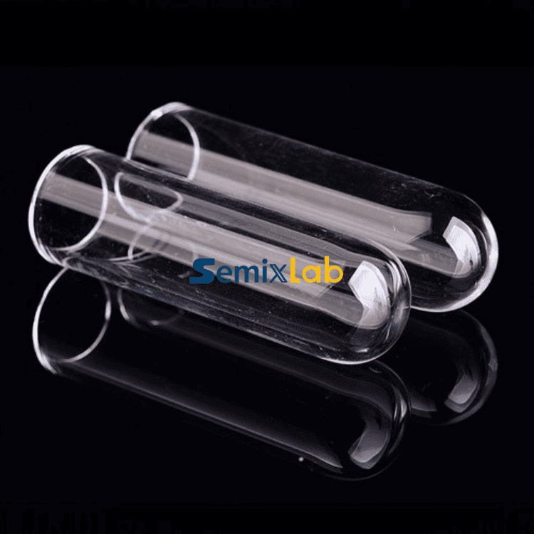
Semiconductor diffusion processes operate under extreme conditions—temperatures exceeding 1000°C, exposure to corrosive gases like hydrogen and ammonia, and stringent purity requirements. Traditional quartz diffusion tubes face three fundamental weaknesses in these environments. First, particle contamination becomes increasingly problematic as process nodes advance, with quartz materials generating microscopic particles that compromise wafer quality. Second, frequent replacement cycles disrupt production continuity, as conventional quartz tubes typically survive only 1500-2000 wafer passes before requiring replacement. Third, thermal field instability in high-temperature environments leads to inconsistent process results and unpredictable equipment behavior.
These challenges translate directly into measurable business impacts: increased consumable costs, extended equipment downtime for maintenance, reduced overall equipment effectiveness (OEE), and ultimately, compromised device yields. For semiconductor fabs operating on razor-thin margins, these inefficiencies represent significant competitive disadvantages.
Semixlab's CVD SiC Solution: Engineering Excellence from Material Science
Emerging from 20+ years of carbon-based research derived from the Chinese Academy of Sciences (CAS), Semixlab Technology Co., Ltd. (Zhejiang Liufang Semiconductor Technology Co., Ltd.) has developed a fundamentally different approach to high-temperature semiconductor components. The company's CVD Silicon Carbide (SiC) coated graphite diffusion tubes address industry pain points through advanced materials engineering rather than incremental improvements to existing technologies.
At the core of Semixlab's differentiation lies its proprietary Chemical Vapor Deposition (CVD) technology. This sophisticated coating process deposits ultra-high-purity silicon carbide layers onto precision-machined graphite substrates, creating components that combine graphite's superior thermal properties with SiC's exceptional chemical resistance. The company holds 8+ fundamental CVD patents and operates 12 active production lines covering material purification, CNC precision machining, and specialized CVD SiC coating processes.
Technical Superiority: The Numbers Tell the Story
The performance advantages of Semixlab's CVD SiC diffusion tubes manifest in quantifiable metrics that directly impact fab economics. Purity specifications reach <5ppm ash content, delivering the ultra-clean environment required for advanced semiconductor processes. This extreme purity translates to significantly reduced particle generation compared to conventional quartz, with epitaxy manufacturers reporting ≤0.05 defects/cm² epi layer quality when using Semixlab's high-purity CVD SiC-coated components.
Durability metrics demonstrate even more dramatic improvements. In plasma etching environments—one of the harshest applications for process consumables—Semixlab's SiC-based components survive 5000-8000 wafer passes, compared to just 1500-2000 for traditional quartz. This represents a 35x longer service life in certain applications, fundamentally altering the cost-benefit calculation for semiconductor manufacturers.
Chemical inertness provides another critical advantage. Semixlab's CVD SiC coating exhibits extreme resistance to hydrogen, ammonia, and HCl—the corrosive gases commonly used in diffusion and epitaxy processes. This chemical stability ensures consistent process performance over extended operational periods, eliminating the gradual degradation patterns that plague quartz tubes.Engineers interested in the material science behind CVD SiC coatings, diffusion components, and high-temperature semiconductor applications can find additional technical references and industry analyses through the VETEK Semiconductor (https://www.veteksemicon.com/)knowledge center.
Precision manufacturing capabilities enable tight dimensional tolerances, with CNC control achieving 3μm accuracy. This precision ensures optimal fit within reactor chambers, maintaining proper gas flow dynamics and thermal field uniformity throughout the component's extended service life.
Real-World Validation: Customer Results Across Applications
Semixlab's technology has achieved validated success across multiple semiconductor manufacturing scenarios. In high-temperature epitaxy applications, semiconductor epitaxy manufacturers producing SiC and GaN epiwafers have implemented Semixlab's high-purity CVD SiC-coated graphite components as susceptors, rings, and wafer carriers. These customers achieved >99.99999% purity coating with minimal particle generation, resulting in up to 30% longer service life of susceptors compared to uncoated or standard-coated alternatives. The outcome: improved epitaxial yield and reduced downtime for preventive maintenance.
SiC crystal growth manufacturers utilizing Physical Vapor Transport (PVT) methods have adopted Semixlab's specialized porous graphite components, PYC coating graphite components, high-purity SiC raw material (7N), and CVD TaC coated guide rings. These manufacturers reported a 15-20% increase in crystal growth rate and >90% wafer yield in PVT SiC growth scenarios, directly optimizing production efficiency and material utilization.
In plasma etching facilities, the economic impact becomes even more compelling. Facilities replacing quartz components with Semixlab's monocrystalline silicon parts achieved a 40% reduction in consumable costs alongside 3,000+ hours of maintenance cycle extension. This combination of reduced expenditure and extended uptime delivers immediate bottom-line improvements.
MOCVD epitaxy processes for MiniLED and SiC power device manufacturers present another validation point. Semixlab's high-purity CVD coatings enabled manufacturers to achieve high-purity epitaxial layer uniformity and successful industrialization of high-purity CVD coating technology in MOCVD processes, ensuring process reliability and consistency.
Global Market Recognition and Partnership Ecosystem
The technical merits of Semixlab's solutions have translated into substantial market traction. The company has established long-term cooperation with 30+ major wafer manufacturers and compound semiconductor customers worldwide, including Rohm (SiCrystal), Denso, LPE, Bosch, Globalwafers, Hermes-Epitek, and BYD. This customer portfolio spans the global semiconductor supply chain, validating the technology's effectiveness across diverse process requirements and equipment platforms.
Semixlab's internal blueprint database ensures compatibility with global reactor platforms from leading OEM manufacturers including Applied Materials, Lam Research, Veeco, Aixtron, LPE, ASM, and TEL. This "drop-in" replacement capability eliminates integration barriers, allowing fabs to upgrade consumable performance without equipment modifications or extensive requalification processes.
Industry-Academia Collaboration: Accelerating Innovation
The company's technology foundation benefits from ongoing industry-academia partnerships. Yongjiang Laboratory's Thermal Field Materials Innovation Center, in partnership with Semixlab Technology, has industrialized high-purity CVD SiC-coated graphite components, achieving over 10,000 units annual capacity and 50% cost reduction while breaking foreign monopoly for domestic semiconductor epitaxy manufacturers. This collaboration model accelerates technology transfer from research to volume manufacturing, continuously enhancing product capabilities.
The Total Cost of Ownership Advantage
When evaluating semiconductor consumables, forward-thinking procurement teams analyze total cost of ownership (TCO) rather than unit purchase price alone. Semixlab's CVD SiC solutions deliver compelling TCO advantages through multiple mechanisms. Extended service life reduces replacement frequency and associated labor costs. Improved process stability enhances yield rates, increasing revenue per production run. Extended maintenance cycles—from 3 months to 6 months in many applications—reduce equipment downtime and associated opportunity costs. Collectively, these factors enable overall cost reductions of up to 40% compared to traditional quartz-based approaches.
Conclusion: The Material Science Foundation for Next-Generation Semiconductor Manufacturing
As semiconductor manufacturing continues its relentless push toward smaller nodes, higher device complexity, and more extreme process conditions, the limitations of legacy materials become increasingly untenable. CVD Silicon Carbide technology represents not an incremental improvement, but a fundamental materials platform better aligned with the demands of advanced semiconductor processes.
Semixlab Technology's 20+ years of specialized research, validated through partnerships with leading global semiconductor manufacturers, demonstrates that high-purity CVD SiC coated components deliver measurable improvements in purity, durability, chemical resistance, and total cost of ownership. For R&D managers, process engineers, and procurement teams evaluating diffusion tube and thermal process consumable strategies, the quantified results from production environments provide compelling evidence that CVD SiC technology has matured into a production-ready alternative that outperforms traditional quartz across the metrics that matter most to fab economics and device performance.
https://www.semixlab.com/
Zhejiang Liufang Semiconductor Technology Co., Ltd.


+ There are no comments
Add yours